

Tests & Services
Explore our comprehensive range of nanoscience services designed to support research, education, and innovation.
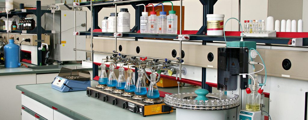
Lab. Tests
Devices
Proof Reading
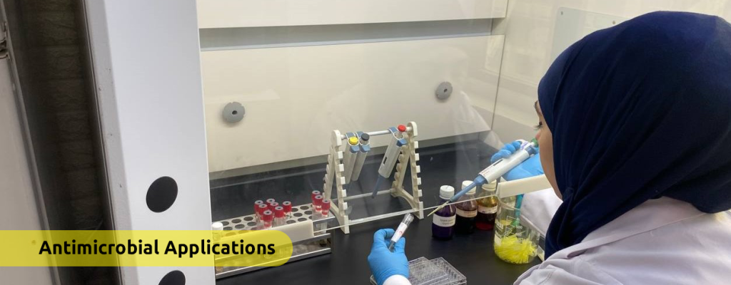
Applications


Our Contributions
Some of the contributions of PNSC to the field of nanotechnology are:
- Published several papers in international journals on topics such as nanomaterials synthesis, characterization, and applications.
- Organized workshops and conferences to promote the exchange of knowledge and collaboration among nanotechnology researchers and experts.
- Participated in national and international projects and networks related to nanotechnology, such as the Arab Nanotechnology Network.
- Trained and educated young scientists and students in the field of nanotechnology and provided them with opportunities to pursue their careers.
PNSC is one of the leading institutes in Iraq and surrounding region that is dedicated to advancing the science and technology of nanoscale phenomena. PNSC aims to contribute to the development of society and the environment through nanotechnology.
While we believe we are more than just numbers, the depth of our laboratories is pretty impressive.

What to Expect During Your Visit
During your visit to Phi-Nano Center, you can expect a streamlined and professional experience, beginning with personalized consultation and sample assessment. Our team ensures accurate testing, clear communication of results, and expert guidance tailored to your research or diagnostic needs.
To maintain Social Distancing you may need to wait outside. Once we have your paper work, we will process you in our system.

Research Stages
A structured workflow from initial concept to final delivery, ensuring precision at every step.
How to Create a Service Request at Phi-Nano Center
- Create a new account if you do not have one, or log in to your existing account.
- Select the required service from the available service list.
- Carefully read all service-specific instructions and comply with the required guidelines.
- Pay the specified fee in advance through the available online payment gateway.
- Track your request through the website until it reaches the completion and delivery stage.
Latest News
test
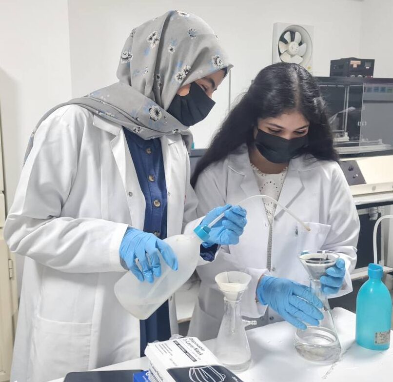
Research Experiments
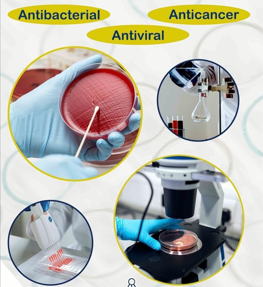
Phi Center for Nanoscience Launches Advanced Services for Evaluating the Biological Applications of Nanoparticles
The Phi Center for Nanoscience has announced the launch of a set of specialized services for assessing the biological effectiveness of synthesized nan...
Read MorePhi-Activities
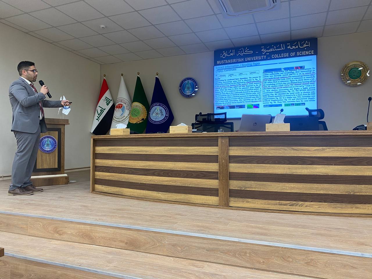
Phi Center for Nanoscience Holds a Scientific Seminar in Collaboration with Al-Mustansiriyah University
The Phi Center for Nanoscience, in cooperation with the Department of Physics – College of Science – Al-Mustansiriyah University, organized a scientif...
Read More