Description
1.1 Basic Principles
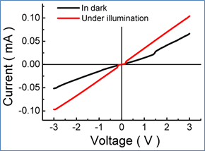
Current voltage characteristics or I-V characteristic of a material means the amount of current a material can carry at a given voltage. It is also a reflection of a material’s resistance to current flow under a given voltage. The resistance of a material is given as the gradient of the graph of current against voltage; a steep gradient indicates a high resistance, while a shallow gradient indicates a low resistance. The current is given by the equation I = V/R, or current equals voltage divided by resistance. The current voltage characteristic of a resistor is a straight line graph passing through the origin. The reason that the quality of a resistor is stated by a % error from a straight line.
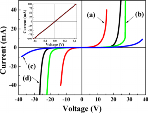
A diode I-V characteristic is a graph of the current through a diode and the voltage across a diode. A diode will only allow current flow when it is forward biased by a voltage higher than its threshold voltage. At this point, it will act as a short circuit and large current will flow through it. If the diode is reverse biased, then a very small reverse saturation current will flow through the diode as a result of charge present in the depletion layer of the diode. The reverse saturation current will increase slightly with reverse voltage.
The final device to be discussed is a field effect transistor or FET. The I-V characteristic for a FET is a graph of the drain current against the drain-source voltage with the gate-source voltage as a parameter. A FET is a voltage controlled device. For a JFET, when the voltage across the diode is zero by shorting Vds to the source, the only current flow will be that of the depletion layer, thus acting as an off switch for the transistor.
1.2 Importance of Understanding I-V Characteristics
It is widely recognized that a fundamental understanding of the I-V characteristics of materials is important for the development of electronic devices. It is no less true for nanomaterials, for which the I-V characteristics can be quite different from those of the bulk. As the size of a material decreases to the nanometer scale, the percentage of atoms located at the surface increases dramatically.
The electronic behavior of a nanomaterial is therefore dominated by the behavior of the surface atoms because electrons and holes have a greater probability of being located at the surface where it costs less in energy to make an excursion into the vacuum or another medium. Since most useful electronic devices rely on the conduction of electrons or holes, the changes in behavior of charge carriers in nanomaterials are of great interest. This type of information is most readily obtained from measurements of the I-V characteristics.
Some other reasons why understanding I-V characteristics is important for nanomaterials are that nanomaterials can exhibit a range of different electrical behaviors. These can include semiconducting, insulating and superconducting behaviors, and it has been shown that the current-voltage characteristics of two samples of material, one semiconducting and one insulating, can look very similar. This makes it hard to gain an initial idea of the electrical behavior of a sample of nanomaterial, and means that more advanced measurements such as tunneling or scanning probe microscopy techniques are needed to fully understand its behavior.
Another reason is that the size and properties of nanomaterials makes them particularly suitable for use in certain types of electronic devices. For example, because of their small size, it is possible to blow billions of nanotubes on to a silicon chip to make a high density random access memory, and nanomaterials are also used in space and military applications where they are exposed to radiation. In this case it has been shown that the electrical behavior of nanomaterials can change when they are irradiated and it is important to be able to monitor the electrical properties in order to assess the suitability of the material for a given application.
