Test Item
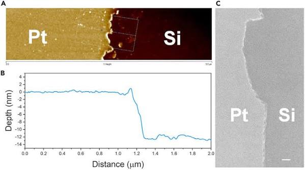
Thickness Measurement via Atomic Force Microscopy
Thin Films, Coatings, and Nanoscale Layers
Phi Nanoscience Center (PNSC)
1. What is AFM Thickness Measurement?
Atomic Force Microscopy is a high-resolution surface-characterization technique that measures the three-dimensional topography of a material by scanning a sharp probe across its surface.
AFM can determine the thickness of thin films, coatings, deposited layers, and nanoscale structures by measuring the vertical height difference between the coated surface and an exposed reference substrate.
Unlike optical methods, AFM does not depend primarily on sample transparency, color, or refractive index. It directly measures surface height and can provide thickness values from the nanometre scale up to the instrument’s available vertical scanning range.
Key Applications
- Thickness measurement of thin films and nanocoatings.
- Measurement of deposited polymer layers.
- Evaluation of spin-coated and dip-coated films.
- Thickness analysis of metallic and metal-oxide coatings.
- Measurement of semiconductor layers.
- Characterization of graphene, graphene oxide, and other two-dimensional materials.
- Measurement of biological films and membranes.
- Evaluation of layer uniformity across different sample positions.
- Measurement of step height produced by masking, scratching, etching, or lift-off.
- Correlation of coating thickness with roughness and morphology.
- Quality control of microfabricated and nanofabricated surfaces.
2. Principle of Operation
AFM thickness measurement is based on determining the height difference between two surface levels:
- The upper surface of the deposited film or coating.
- The lower surface of the exposed substrate or underlying layer.
Simplified Measurement Procedure
- Step 1: A clear step or boundary is created between the coating and the exposed substrate.
- Step 2: The sample is mounted securely on the AFM stage.
- Step 3: A sharp AFM probe scans across both the coated and uncoated regions.
- Step 4: The vertical movement of the probe is recorded as a three-dimensional topographic image.
- Step 5: A line profile is drawn across the step boundary.
- Step 6: The vertical distance between the two surface levels is calculated.
- Step 7: Several line profiles or scan locations are analyzed to determine the average thickness and variation.
The film thickness is expressed as:
[
t = Z_{\text{film}}-Z_{\text{substrate}}
]
Where:
- (t) is the film thickness.
- (Z_{\text{film}}) is the average height of the coated region.
- (Z_{\text{substrate}}) is the average height of the exposed substrate.
3. Why is a Step Edge Required?
AFM does not normally determine the absolute thickness of a continuous film when the entire scanned surface is coated.
A measurable boundary must be present between the film and a reference surface. This boundary is commonly called a step edge.
The step can be produced using:
- Partial masking before film deposition.
- Mechanical scratching after deposition.
- Selective chemical removal.
- Lithographic patterning.
- Lift-off processing.
- Partial coating of the substrate.
- Etching of a selected region.
- Natural film boundaries or exposed substrate areas.
Without an exposed reference surface or known lower layer, AFM can measure surface roughness and morphology but may not determine the total film thickness directly.
4. Common Methods for Preparing a Thickness Step
Masking Method
Part of the clean substrate is covered before deposition using suitable tape, a shadow mask, or another removable barrier.
After deposition, the mask is carefully removed, leaving:
- A coated region.
- An uncoated substrate region.
- A distinct boundary between them.
This is generally the preferred method because it avoids damaging the substrate or coating after deposition.
Scratch Method
A narrow region of the coating is removed mechanically to expose the substrate.
Suitable tools may include:
- A clean sharp blade.
- A fine needle.
- A specialized scratching tool.
- A hard probe compatible with the film and substrate.
The scratch must remove the coating completely without deeply damaging the substrate.
Chemical Removal
A selected part of the film is removed using a solvent or chemical reagent that dissolves the coating without attacking the substrate.
This method is suitable only when the chemical compatibility of the film and substrate is well understood.
Lithography or Lift-Off
A patterned step is produced using a resist, mask, or microfabrication process. This approach is useful for controlled and well-defined nanoscale or microscale structures.
5. Suitable Materials
AFM thickness measurements may be performed on:
- Metallic thin films.
- Metal-oxide layers.
- Semiconductor coatings.
- Polymer films.
- Composite coatings.
- Sol–gel films.
- Spin-coated layers.
- Dip-coated layers.
- Spray-coated films.
- Electrodeposited coatings.
- Chemical-vapor-deposited layers.
- Physical-vapor-deposited layers.
- Graphene and graphene oxide.
- Two-dimensional materials.
- Self-assembled monolayers.
- Biomaterial coatings.
- Membranes.
- Photoresist layers.
- Protective and functional coatings.
The sample must be mechanically stable and compatible with AFM scanning.
6. Information You Will Receive in Your Report
- Two-Dimensional AFM Image: A top-view map of the scanned region.
- Three-Dimensional AFM Image: A three-dimensional representation of the surface and step edge.
- Line-Profile Graph: A graph showing height as a function of lateral distance.
- Average Film Thickness: Calculated from the coated and uncoated surface levels.
- Minimum and Maximum Step Height: When multiple measurements are performed.
- Standard Deviation: Used to represent thickness variation between measurements.
- Scan Size: The dimensions of the analyzed AFM area.
- Scanning Mode: Contact, tapping, or another available mode.
- Surface Roughness: Roughness parameters may be provided when requested.
- Measurement Locations: Number and positions of the analyzed line profiles.
- Observation Report: A brief description of step quality, coating uniformity, roughness, defects, and measurement reliability.
- Digital Data: Images and profile data suitable for additional analysis.
Example Result
A clear step boundary was observed between the coated and uncoated regions. The mean film thickness calculated from five line profiles was 186.4 ± 7.2 nm. Minor height variation was attributed to surface roughness and non-uniform coating deposition near the step edge.
7. Thickness Calculation Methods
Single-Line Profile
A single profile is drawn perpendicular to the coating boundary. The height difference between the two plateaus is calculated.
This method is suitable for:
- Preliminary measurements.
- Smooth films.
- Well-defined step edges.
- Relatively uniform coatings.
However, a single profile may not represent the entire sample.
Multiple-Line Profiles
Several parallel or distributed profiles are measured across the step edge.
This method provides:
- Average thickness.
- Standard deviation.
- Thickness uniformity.
- Improved measurement reliability.
Area-Averaging Method
The average height of a selected coated area is compared with the average height of a selected uncoated area.
[
t=\bar{Z}{\text{coated}}-\bar{Z}{\text{substrate}}
]
This method can reduce the effect of individual surface peaks, valleys, particles, and local roughness.
Histogram Analysis
Height-distribution histograms may show two populations corresponding to:
- The substrate level.
- The coating level.
The difference between the two main height populations may be used to estimate film thickness when the step is clear and the surfaces are sufficiently uniform.
8. Sample Preparation Guide
Sample TypeRecommended PreparationThin Film on a Flat SubstrateCreate a masked or scratched region that exposes the original substrate.Spin-Coated FilmMask a small strip before coating or carefully remove a narrow region after coating.Metallic CoatingUse a deposition mask or controlled scratching method to expose the substrate.Polymer FilmUse masking or remove part of the film using a compatible solvent.Graphene or Two-Dimensional MaterialProvide an area containing both the deposited layer and exposed substrate.Multilayer CoatingExpose the required underlying layer and clearly identify which layer thickness is required.Soft or Biological FilmAvoid aggressive scratching; use masking or selective deposition where possible.Rough CoatingPrepare a wide, clear step and measure several positions to account for roughness.
Essential Requirements
- The sample should be flat.
- The film must be firmly attached to the substrate.
- The step edge should be clearly visible or locatable.
- Both coated and uncoated regions must fit within a practical AFM scan area.
- The exposed substrate must not be deeply scratched or deformed.
- The sample must be clean, dry, and free from loose particles.
- The sample should be securely mounted without bending.
- The coating and substrate materials should be identified.
- The expected thickness range should be provided when known.
9. Recommended Step Geometry
For reliable analysis, the prepared step should:
- Extend across enough of the scan area to allow profile measurements.
- Contain clear coated and uncoated plateaus.
- Have minimal debris along the edge.
- Avoid severe cracking or peeling.
- Avoid deep grooves in the substrate.
- Be sufficiently narrow to allow both levels to appear in one scan.
- Be approximately perpendicular to the intended profile direction.
- Be located away from sample edges whenever possible.
An excessively rough or damaged step may introduce uncertainty into the thickness result.
10. Understanding Your Results
Clear Step Profile
An ideal profile contains:
- A relatively flat substrate region.
- A transition boundary.
- A relatively flat coated region.
- A measurable vertical difference between the two levels.
The vertical difference represents the apparent coating thickness.
Surface Roughness
Both the film and substrate may contain surface peaks and valleys. Therefore, the thickness should preferably be determined from average surface levels rather than from isolated points.
High roughness may cause:
- Variation between line profiles.
- Uncertainty in defining the surface level.
- Larger standard deviation.
- Difficulty distinguishing the true step height.
Edge Accumulation
Some deposition methods may produce a thicker region near the mask boundary. This is sometimes called an edge bead or accumulation zone.
Thickness should be measured sufficiently far from this region when the objective is to determine the representative bulk-film thickness.
Incomplete Film Removal
If the scratched or chemically treated region still contains coating residue, the measured step height will underestimate the true thickness.
Substrate Damage
If scratching removes part of the substrate, the measured depth will overestimate the coating thickness.
Film Deformation
Soft films may deform under the AFM probe, particularly in contact mode. This can lead to an underestimated thickness.
A low-force or tapping-mode measurement may be preferable for delicate films.
11. Surface Roughness Parameters
Thickness measurement can be combined with surface-roughness analysis.
Common roughness parameters include:
Average Roughness
[
R_a=\frac{1}{N}\sum_{i=1}^{N}|Z_i-\bar{Z}|
]
The average absolute deviation of surface heights from the mean level.
Root-Mean-Square Roughness
[
R_q=\sqrt{\frac{1}{N}\sum_{i=1}^{N}(Z_i-\bar{Z})^2}
]
RMS roughness is more sensitive to high peaks and deep valleys than average roughness.
Peak-to-Valley Height
The vertical distance between the highest and lowest measured points in the selected area.
Reporting roughness alongside thickness can help determine whether the measured layer is smooth, uniform, particulate, porous, or defective.
12. Advantages of AFM Thickness Measurement
- Nanometre-scale vertical sensitivity.
- Direct surface-height measurement.
- Three-dimensional surface imaging.
- Minimal sample preparation.
- No conductive coating is required.
- Suitable for conductive and non-conductive materials.
- Can measure thickness and roughness in the same scan.
- Applicable to transparent and opaque films.
- Useful for very thin layers that may be difficult to measure by mechanical methods.
- Allows localized measurements on selected surface areas.
- Provides digital line profiles and statistical analysis.
13. Limitations
- A clear reference step is usually required.
- AFM measures local thickness over a relatively small area.
- The measured region may not represent the entire sample.
- Very rough surfaces can increase measurement uncertainty.
- Loose, weakly bonded, or highly porous coatings may be damaged during scanning.
- Soft films may deform under probe forces.
- Thick films may exceed the available vertical scan range.
- Curved samples are difficult to measure accurately.
- Contamination or particles near the step can distort the profile.
- Tip geometry may broaden narrow lateral features.
- AFM does not directly identify the chemical composition of the layer.
- Scratching may damage the substrate and produce an incorrect thickness.
- Layer thickness cannot normally be obtained from a fully continuous coating without a reference level.
- Thermal drift, vibration, and improper leveling can affect the result.
For macroscopic coatings or films thicker than the AFM vertical range, profilometry, cross-sectional microscopy, or another thickness method may be more suitable.
14. Frequently Asked Questions
Can AFM measure film thickness?
Yes. AFM measures the vertical step between a coated region and an exposed substrate or underlying layer.
Is a scratch required?
Not always. A step can be created by masking, etching, lift-off, partial coating, or another controlled method. Masking before deposition is often preferable to scratching afterward.
Can AFM measure a fully coated sample?
AFM can measure its roughness and surface morphology, but total coating thickness generally cannot be determined unless an exposed reference surface or known step is available.
What thickness range can be measured?
The measurable range depends on the instrument’s vertical scanner and the sample geometry. AFM is particularly useful for nanometre-scale and thin micrometre-scale films.
Can graphene thickness be measured?
Yes. AFM is widely used to measure the height of graphene, graphene oxide, and other two-dimensional materials relative to an exposed substrate.
However, apparent height may be affected by adsorbed water, contamination, substrate interactions, and measurement conditions.
Can soft polymer films be measured?
Yes, but low-force or tapping-mode scanning may be required to minimize surface deformation.
Can coating thickness and roughness be obtained together?
Yes. The step height can provide film thickness, while selected coated areas can be analyzed for surface roughness.
Can AFM measure multilayer films?
Yes, provided that the required layer boundaries or reference levels are exposed and clearly distinguishable.
How many profiles should be measured?
At least three to five line profiles at different positions are recommended. Additional measurements may be needed for rough or non-uniform coatings.
Does the scratch depth equal film thickness?
Only when the coating is completely removed and the underlying substrate is not damaged.
Can powder samples be measured for thickness?
Loose powders do not have a continuous film thickness. They may be analyzed for particle morphology and height after deposition on a suitable substrate.
Can AFM determine coating uniformity?
It can evaluate local thickness variation and roughness at several scanned positions. Large-area uniformity requires measurements at multiple locations.
How much sample is required?
A small flat specimen is generally sufficient, provided that it can be mounted securely and contains both coated and reference regions.
How long does the analysis take?
Basic thickness measurement may require approximately 1–2 hours after receiving a properly prepared sample.
Additional time may be required for:
- Multiple scan locations.
- Several sample groups.
- Roughness analysis.
- Multilayer measurements.
- Statistical analysis.
- Detailed three-dimensional image processing.
15. Common Sources of Measurement Error
- Incomplete removal of the film.
- Excessive scratching into the substrate.
- Debris deposited inside the scratch.
- Tilt between coated and uncoated surfaces.
- Surface contamination.
- Poor image leveling or flattening.
- Incorrect selection of reference areas.
- Tip contamination or wear.
- Thermal drift.
- Sample movement.
- Film deformation.
- High surface roughness.
- Measuring within an edge-bead region.
- Using only one profile on a non-uniform film.
To improve reliability, measurements should be repeated across several profiles and, when possible, at several sample positions.
16. Recommended Reporting Format
An AFM thickness report should include:
- Sample name or code.
- Film and substrate materials.
- Deposition method.
- Step-preparation method.
- AFM scanning mode.
- Scan size.
- Image resolution.
- Scan rate, when required.
- Probe information, when available.
- Raw and processed topographic images.
- Three-dimensional surface image.
- Line-profile positions.
- Individual thickness values.
- Mean film thickness.
- Standard deviation.
- Surface roughness values, when requested.
- Image-processing and leveling method.
- Notes regarding edge quality, debris, roughness, or film damage.
Example Reporting Table
SampleScan SizeNumber of ProfilesMean ThicknessStandard DeviationSurface ObservationPolymer Film A20 × 20 µm²592.6 nm4.1 nmSmooth and uniformMetal-Oxide Film B50 × 50 µm²6318.4 nm16.7 nmModerate roughnessNanocomposite Film C30 × 30 µm²51.24 µm0.09 µmParticulate surface
17. Recommended Complementary Analyses
Depending on the sample and research objective, AFM thickness measurement may be combined with:
- Stylus Profilometry: For larger-area step-height and thickness measurements.
- Optical Profilometry: For non-contact three-dimensional surface mapping.
- Ellipsometry: For very thin, smooth, optically uniform films.
- Cross-Sectional SEM: For direct observation of coating thickness and internal structure.
- Transmission Electron Microscopy: For nanoscale multilayer and interface analysis.
- Optical Microscopy: For identifying the step location and macroscopic coating defects.
- FESEM: For surface morphology and cross-sectional imaging.
- EDS Analysis: For elemental analysis of the coating and substrate.
- X-ray Reflectivity: For thickness, density, and roughness of thin films.
- FTIR Spectroscopy: For functional-group identification.
- X-ray Diffraction: For crystalline-phase and structural analysis.
- Contact-Angle Measurement: For evaluating the effect of film thickness and surface morphology on wettability.
18. References
- [1] Eaton, P., & West, P. (2010). Atomic Force Microscopy. Oxford University Press.
- [2] Butt, H. J., Cappella, B., & Kappl, M. (2005). Force Measurements with the Atomic Force Microscope: Technique, Interpretation and Applications. Surface Science Reports, 59, 1–152.
- [3] Binnig, G., Quate, C. F., & Gerber, C. (1986). Atomic Force Microscope. Physical Review Letters, 56, 930–933.
- [4] ISO 25178. Geometrical Product Specifications—Surface Texture: Areal.
- [5] ISO 4287. Geometrical Product Specifications—Surface Texture: Profile Method.
- Internal Source: Phi Nanoscience Center provides AFM thickness, step-height, three-dimensional topography, and surface-roughness measurements for thin films, coatings, nanostructures, polymers, semiconductors, and advanced materials.
19. Request This Test
To request AFM Thickness and Step-Height Measurement or any of our other analytical services, please complete the Sample Testing Request Form.