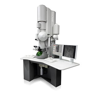
TEM (Transmission Electron Microscopy)
Phi Nanoscience Center (PNSC)
1. What is TEM?
Transmission Electron Microscopy (TEM) is a powerful imaging technique that uses a high-energy electron beam transmitted through an ultra-thin sample to image the internal structure, crystallography, and fine morphology of materials at the atomic scale [1].
TEM is essential for nanotechnology research because it provides true physical size (not hydrodynamic), reveals crystal lattice fringes, and shows internal defects that other techniques cannot see.
Key Applications in Nanomaterials Research:
- Determining the true size, shape, and size distribution of individual nanoparticles (not agglomerates).
- Visualizing crystal lattice fringes (interplanar spacing) to identify crystalline phases and orientation.
- Observing defects, dislocations, grain boundaries, and core-shell structures.
- Selected Area Electron Diffraction (SAED) for crystal structure determination (amorphous vs. polycrystalline vs. single crystal).
- Characterizing quantum dots, nanowires, nanotubes, and 2D materials (e.g., graphene).
2. Principle of Operation (Simplified)
- Step 1: A high-energy electron beam (typically 80-300 kV) is transmitted through an ultra-thin sample (< 100 nm thick).
- Step 2: Electrons interact with the sample as they pass through. Some electrons are scattered (by atoms, defects, or crystal planes), others are transmitted without interaction.
- Step 3: An electromagnetic lens system focuses the transmitted electrons to form:
- Bright-Field (BF) Image: Regions that scatter electrons strongly (e.g., dense or thick areas) appear dark; regions that transmit electrons appear bright.
- Selected Area Electron Diffraction (SAED) Pattern: A pattern of spots or rings from which crystal structure and orientation can be determined.
- Step 4: A detector captures the image or diffraction pattern [2].
- High-Resolution TEM (HRTEM): Uses phase contrast from the transmitted and diffracted beams to image atomic lattice planes directly (crystal fringes).
3. Information You Will Receive in Your Report
Technique
Information Provided
Bright-Field TEM Images
Images showing the size, shape, dispersion, and internal structure of your nanoparticles.
Particle Size Histogram
Average particle size, standard deviation, and size distribution (from image analysis of multiple particles).
High-Resolution TEM (HRTEM) Images
Images showing crystal lattice fringes. Lattice spacing (d-spacing) can be measured.
Selected Area Electron Diffraction (SAED) Pattern
Ring pattern (polycrystalline) or spot pattern (single crystal). Used to determine crystal structure and identify phases.
Measurement Report
Average particle size, d-spacing values, crystal structure interpretation, and any observed defects or features.
4. Sample Preparation Guide
This is the most critical and challenging part of TEM. The sample must be electron-transparent (< 100 nm thick).
Sample Type
Preparation Method
Nanoparticles (Powder)
Disperse a small amount of powder in a volatile solvent (e.g., ethanol, isopropanol, or deionized water). Sonicate for 5-10 minutes to break up agglomerates. Drop-cast 2-3 drops onto a TEM grid (e.g., holey carbon film on a copper grid). Dry under an IR lamp or in a desiccator.
Liquid Suspension
Same as powder. Dilute the suspension if it is too concentrated (to avoid clumping).
Cross-Section of Thin Film
Complex and specialized. Requires embedding, cutting, grinding, polishing, and ion milling (e.g., FIB or precision ion polishing). This is typically outsourced.
2D Material (e.g., graphene, MoS₂)
Transfer the 2D material onto a TEM grid directly.
Biological Samples
Require fixation, staining, embedding, and ultra-microtomy. Specialized service.
Important Notes:
- Particle Size: Individual particles should be clearly separated (not touching or overlapping) for accurate size measurement.
- Solvent Choice: Use a volatile solvent that evaporates quickly (water is acceptable but dries slower).
- Grid Type: Holey carbon film on a copper grid is standard for nanoparticles. For very small particles (< 5 nm), use an ultrathin carbon film or graphene oxide support.
- Samples must be completely dry before insertion into the TEM (vacuum is < 10⁻⁵ Pa).
5. Understanding Your Results (Guide to Interpretation)
Bright-Field TEM Images:
- Particle Size: The true physical size of individual particles (this will be smaller than DLS values, which measure the hydrodynamic diameter including the solvation layer).
- Particle Morphology: Are the particles spherical, rod-like, platelet, cubic, or irregular? Are they uniform in shape?
- Dispersion: Are the particles well-separated (individual) or agglomerated (clumped together)?
- Internal Structure: Can you see a darker core and lighter shell (core-shell structure)? Are there voids or defects inside the particles?
High-Resolution TEM (HRTEM):
- Lattice Fringes: Parallel lines within a nanoparticle. The spacing between fringes (d-spacing) corresponds to specific crystal planes.
- Measuring d-Spacing: Use ImageJ or the microscope's software to measure the distance between fringes (nm). Compare to standard XRD databases to identify the crystal phase (e.g., d = 0.235 nm for Ag (111) planes).
- Crystallinity: Regular, parallel fringes throughout the particle = highly crystalline. Disordered fringes or amorphous regions = poor crystallinity.
Selected Area Electron Diffraction (SAED):
- Sharp Rings: Polycrystalline material (many small crystals randomly oriented). The ring diameters correspond to d-spacings.
- Sharp Spots: Single crystal (the beam is on a single, oriented crystal).
- Diffuse Rings (Halo): Amorphous material (no long-range order).
- Compare ring/spot positions to a diffraction database to identify the crystal structure (e.g., FCC, BCC, etc.).
6. Frequently Asked Questions (FAQ)
Question
Answer
What is the difference between TEM and SEM?
SEM images the surface of a bulk sample (like looking at the outside of a ball). TEM images the internal structure of an ultra-thin sample (like looking at a very thin slice through the ball). TEM provides much higher resolution (atomic scale vs. nanometer scale).
What resolution can TEM achieve?
High-resolution TEM (HRTEM) can resolve individual atomic planes (0.1-0.2 nm). Standard TEM resolution is ~0.2-0.5 nm.
How much sample do you need?
A tiny amount (micrograms) of powder or a small piece of material that can be thinned to < 100 nm.
Is sample preparation difficult?
Yes, it is the most challenging part of TEM. Nanoparticles are relatively easy (drop-casting). Cross-sections are very difficult and costly.
Can you do elemental analysis (EDX) in TEM?
Yes, we offer TEM-EDX as an add-on service (requires specialized holders and longer analysis time). Please inquire.
Can you measure particle size from TEM images?
Yes, we can provide a particle size histogram (average size, standard deviation, distribution) as an optional add-on service.
How long will the analysis take?
3-7 days from sample receipt, depending on the complexity of sample preparation. Simple nanoparticle dispersions are faster.
Is TEM expensive?
Yes, it is one of the more expensive techniques due to the instrument cost and sample preparation complexity.
7. References
- [1] Williams, D. B., & Carter, C. B. (2009). Transmission Electron Microscopy: A Textbook for Materials Science (2nd ed.). Springer.
- [2] Reimer, L., & Kohl, H. (2008). Transmission Electron Microscopy: Physics of Image Formation (5th ed.). Springer.
- Internal Source: Phi Nanoscience Center (PNSC) offers TEM imaging for nanoparticle samples (sample preparation is the user's responsibility).
8. Request This Test
To request TEM analysis or any of our other services, please complete the Sample Testing Request Form using the link below. We will contact you within 24 hours to discuss your sample, preparation requirements, and specific imaging needs (e.g., bright-field only, HRTEM, SAED, or particle size analysis).