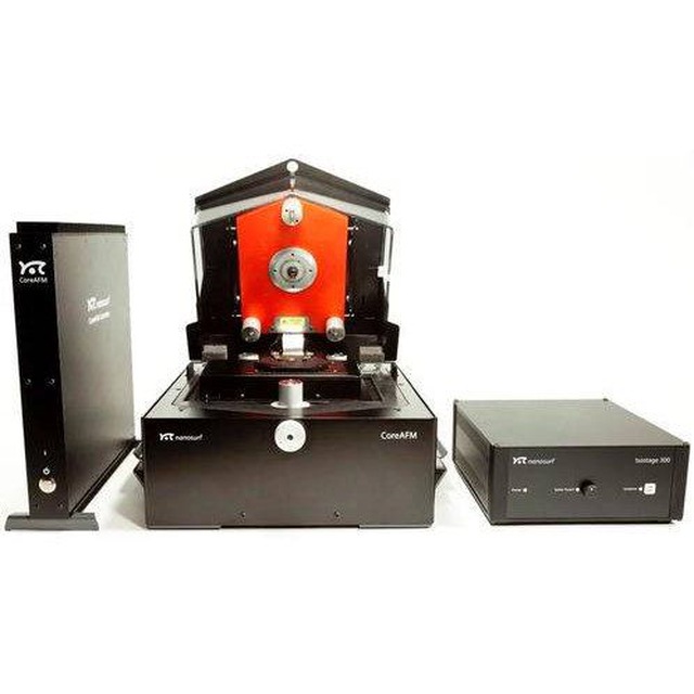
Atomic Force Microscopy (AFM)
Phi Nanoscience Center (PNSC)
1. What is Atomic Force Microscopy (AFM)?
Atomic Force Microscopy (AFM) is a high-resolution scanning probe microscopy technique that is used to image and measure the surface topography, roughness, and mechanical properties of materials at the nanometer to atomic scale. Unlike electron microscopes (SEM, TEM), AFM uses a sharp mechanical probe to "feel" the surface, allowing it to image non-conductive samples without any special coating [1].
AFM is an essential tool for nanotechnology research because it provides true 3D topographic data, measures surface roughness quantitatively, and can probe mechanical properties (e.g., hardness, adhesion, modulus) at the nanoscale.
Key Applications in Nanomaterials Research:
- 3D Surface Topography: Visualizing nanoparticles, nanofibers, thin films, and biological samples (cells, proteins, DNA) in their natural state.
- Quantitative Surface Roughness (Ra, Rq, Rz): Measuring roughness parameters over a defined scan area.
- Particle Size and Height: Determining the true vertical height of nanoparticles, which is often different from lateral dimensions.
- Thin Film Characterization: Measuring film thickness (by scratching a line) and studying film morphology and pinholes.
- Mechanical Property Mapping (PeakForce QNM): Mapping nanomechanical properties such as modulus (stiffness), adhesion, deformation, and energy dissipation simultaneously with topography [2].
2. Principle of Operation (Simplified)
- Step 1: A sharp tip (radius of curvature < 10 nm) attached to the end of a flexible cantilever is brought into close proximity with the sample surface.
- Step 2: The tip is raster-scanned (moved back and forth) across the surface.
- Step 3: As the tip encounters surface features (peaks and valleys), the cantilever bends (deflects) due to forces between the tip and the sample (van der Waals forces, electrostatic forces, etc.) .
- Step 4: A laser beam is reflected off the back of the cantilever into a position-sensitive photodetector (PSPD), which measures the cantilever's deflection with sub-nanometer precision.
- Step 5 (Feedback Loop): A feedback system maintains a constant force between the tip and the sample by moving the scanner up or down (Z-axis). This vertical movement is recorded and used to generate a 3D topographic image.
Common Imaging Modes:
Mode
Description
Best For
Contact Mode
Tip drags in constant contact with the surface.
Hard, firmly attached samples in air or liquid. High resolution but can damage soft samples.
Tapping Mode (Intermittent Contact)
Cantilever oscillates near its resonance frequency; tip lightly taps the surface intermittently.
Soft, delicate, and loosely bound samples (polymers, biological samples, nanoparticles). Minimizes lateral forces. Most common mode for nanomaterials.
PeakForce Tapping® (ScanAsyst)
An advanced version of Tapping Mode where the peak force (maximum repulsive force) is controlled directly.
Provides high-resolution imaging with extremely low forces. Ideal for very soft or fragile samples .
3. Information You Will Receive in Your Report
Information
How It Benefits Your Research
2D and 3D Topographic Images: High-resolution images of the sample surface.
Visualizes surface morphology (features, pores, particles, agglomerates) in 3D.
Surface Roughness Parameters (Ra, Rq, Rz): Quantitative roughness values over a defined area.
Essential for quality control, comparing surface treatments, and characterizing thin films.
Particle Size and Height Analysis: The average height of nanoparticles (nm) and their distribution.
Provides the true vertical size of nanoparticles (different from lateral size from SEM).
Section Analysis: A cross-sectional profile of the surface along a user-defined line.
Measures step heights, particle heights, and feature depths.
Film Thickness Measurement: The height difference between a scratched line and the substrate.
Critical for quality control of deposited thin films and coatings.
Nanomechanical Property Maps (Optional): Maps of modulus (DMT modulus), adhesion, deformation, and energy dissipation.
Relates topography to material properties; identifies different phases and contaminants .
Scan Conditions Report: Scan size, scan rate, setpoint, and mode used.
Ensures reproducibility.
4. Sample Preparation Guide
AFM has relatively simple sample preparation compared to electron microscopy, but it is critical for obtaining high-quality images.
Sample Type
Preparation Method
Important Notes
Powder / Nanoparticles
Spin-Coating or Drop-Casting: Disperse a small amount of powder in a volatile solvent (e.g., ethanol, isopropanol). Sonicate to break up agglomerates. Spin-coat or drop-cast a few drops onto a clean, flat substrate (e.g., freshly cleaved mica, silicon wafer, or HOPG). Dry under an IR lamp.
Critical: The surface must be very flat and clean. Too much material will cause agglomerates; too little will have few particles to image.
Thin Film / Coated Wafer
Clean the surface with a gentle gas jet (N₂ or Ar) to remove loose dust. Mount the wafer on the AFM sample holder using double-sided tape or a magnetic puck.
For accurate roughness measurement, the sample must be free of dust and scratches.
Liquid / Biological Samples (Cells, Proteins, DNA)
Immobilization: The sample must be immobilized on a suitable substrate (e.g., freshly cleaved mica, functionalized glass). Cells are typically fixed and dried or imaged in liquid.
AFM can image in liquid using a fluid cell. This is essential for biological samples in their native state.
Solid / Metal / Ceramic
Clean the surface with a suitable solvent (e.g., IPA, acetone) to remove surface grease. Mount using a magnetic puck or double-sided tape.
For bulk analysis, the sample must be flat and rigid. A surface roughness of < 1 µm is preferred.
General Requirements:
Requirement
Detail
Maximum Sample Size
Typically up to 100 mm diameter; height < 15 mm (varies by instrument).
Surface Flatness
For topographic imaging, the overall sample tilt should be minimal. Height variations should be within the Z-range of the scanner (typically < 5-10 µm for high-resolution imaging).
Cleanliness
The sample surface must be free of dust, grease, and loose particles.
5. Understanding Your Results (Guide to Interpretation)
AFM Images (Topography):
- Color Scale: The color scale (typically from dark to light) represents height (Z-axis). Dark areas are low (valleys), and light areas are high (peaks).
- Particle Morphology: The 3D shape of nanoparticles (spherical, rod-like, irregular).
- Agglomeration: Are the particles well-dispersed (individual) or clumped together (agglomerates)?
- Surface Defects: Visible features like pits, cracks, voids, or contamination.
Surface Roughness Parameters:
- Ra (Average Roughness): The arithmetic average of the absolute height deviations from the mean line. The most commonly reported parameter. A lower Ra indicates a smoother surface.
- Rq (Root Mean Square Roughness): The standard deviation of the height distribution. More sensitive to high peaks and deep valleys than Ra.
- Rz (Maximum Height): The sum of the highest peak and the deepest valley within the evaluation length.
Section Analysis:
- Particle Height: The vertical distance from the substrate baseline to the top of a particle. This is the true height of the particle, often different from the lateral (x-y) size measured by SEM.
- Step Height: For a film, the height difference between the top of the film and the exposed substrate (in a scratch) gives the film thickness.
Artifacts (Common Problems):
Artifact
Cause
Solution
Tip Artifacts (Double Images)
A dull or contaminated tip images itself, creating repeated or "ghost" features.
Clean or replace the tip.
Vibration Noise
High-frequency ripples or waves across the image.
Isolate the instrument from vibrations; image during low-activity hours.
Scanning Artifacts
Lines, streaks, or bowing.
Adjust scan parameters (rate, gains); clean the tip.
6. Frequently Asked Questions (FAQ)
Question
Answer
What is the resolution of AFM?
Lateral (x-y) resolution: 1-10 nm (tip-dependent). Vertical (z) resolution: < 0.1 nm (atomic scale).
What is the difference between AFM and SEM?
AFM provides true 3D topographic data and can measure nanomechanical properties. SEM provides high-resolution 2D images with a much larger field of view but cannot easily measure vertical height quantitatively. AFM can image non-conductive samples without coating.
Can AFM measure true height?
Yes. AFM provides quantitative height (z) data directly. SEM images are 2D projections and cannot easily measure vertical height without special techniques.
Do I need to coat my sample for AFM?
No. AFM works on both conductive and non-conductive samples. No coating is required.
Can AFM image samples in liquid?
Yes. Using a fluid cell, AFM can image samples in their native liquid environment. This is essential for biological samples (cells, proteins) and for studying dynamic processes.
How much sample do you need?
A small piece of material or a coated substrate of at least 5 x 5 mm is sufficient. For powders, a small amount (a few mg) is enough.
How long will the analysis take?
2-4 days from sample receipt, depending on the number of scan areas and the complexity of data analysis.
7. References
- [1] Binnig, G., Quate, C. F., & Gerber, C. (1986). Atomic force microscope. Physical Review Letters, 56(9), 930-933.
- [2] Eaton, P., & West, P. (2010). Atomic Force Microscopy. Oxford University Press.
- Internal Source: Phi Nanoscience Center (PNSC) offers AFM for high-resolution 3D topography, roughness measurement, and nanomechanical property mapping.
8. Request This Test
To request AFM analysis or any of our other services, please complete the Sample Testing Request Form using the link below. We will contact you within 24 hours to discuss your sample and specific imaging requirements.