Test Item
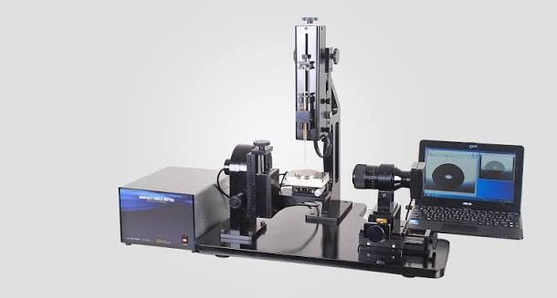
Contact Angle Measurement
20000.00 IQD- Category : Tests
- Group : Nanotechnology Tests
Wettability and Surface Properties
Phi Nanoscience Center (PNSC)
1. What is Contact Angle Measurement?
Contact angle measurement is a surface-characterization technique used to evaluate the wettability of solid materials. It measures the angle formed at the boundary where a liquid droplet, a solid surface, and the surrounding air meet.
The contact angle provides important information about how strongly a liquid interacts with a surface. It is commonly used to determine whether a surface is hydrophilic, hydrophobic, highly wettable, or poorly wettable.
For water droplets:
- A low contact angle indicates good surface wetting and hydrophilic behavior.
- A high contact angle indicates poor wetting and hydrophobic behavior.
- A contact angle near or above 150° may indicate superhydrophobic behavior, provided that suitable droplet adhesion and hysteresis measurements support this classification.
Key Applications in Materials and Nanotechnology Research:
- Evaluating the wettability of metals, polymers, glass, ceramics, and composite materials.
- Studying hydrophilic and hydrophobic surface behavior.
- Assessing surface modification and functionalization.
- Evaluating thin films, nanocoatings, and protective coatings.
- Studying corrosion-resistant and anti-fouling surfaces.
- Examining biomaterials and implant surfaces.
- Assessing surface cleanliness and contamination.
- Comparing treated and untreated samples.
- Evaluating adhesion behavior before painting, coating, printing, or bonding.
- Estimating surface free energy using multiple test liquids.
- Studying water-repellent and self-cleaning materials.
- Evaluating the effect of plasma treatment, oxidation, etching, polishing, or chemical treatment.
2. Principle of Operation (Simplified)
- Step 1: The solid sample is placed horizontally on the instrument stage.
- Step 2: A controlled liquid droplet, commonly deionized water, is deposited onto the sample surface using a microsyringe or automatic dosing system.
- Step 3: A camera captures a side-view image of the droplet.
- Step 4: Image-analysis software identifies the droplet profile and baseline.
- Step 5: The angle between the liquid–solid interface and the tangent to the droplet profile is calculated.
- Step 6: Measurements are repeated at several positions to evaluate surface uniformity and calculate an average value.
The contact angle results from the balance between the surface and interfacial tensions of the solid, liquid, and surrounding atmosphere.
Young’s Equation
For an ideal, smooth, rigid, chemically homogeneous surface at equilibrium:
[
\gamma_{SV} = \gamma_{SL} + \gamma_{LV}\cos\theta
]
Where:
- (\gamma_{SV}): Solid–vapor surface tension.
- (\gamma_{SL}): Solid–liquid interfacial tension.
- (\gamma_{LV}): Liquid–vapor surface tension.
- (\theta): Equilibrium contact angle.
Real surfaces may be rough, porous, chemically heterogeneous, or absorbent. Therefore, the measured angle is often an apparent contact angle rather than an ideal equilibrium value.
3. Types of Contact Angle Measurements
Static Contact Angle
A droplet of fixed volume is placed on the sample surface, and the contact angle is measured after a specified time.
This is the most common method for routine wettability evaluation and comparison between samples.
Advancing Contact Angle
The droplet volume is gradually increased. The largest stable angle observed before the contact line advances is recorded as the advancing contact angle.
This measurement reflects the less-wettable regions of the surface.
Receding Contact Angle
The droplet volume is gradually reduced. The smallest stable angle observed before the contact line recedes is recorded as the receding contact angle.
This measurement is sensitive to surface defects, contamination, roughness, and liquid adhesion.
Contact Angle Hysteresis
Contact angle hysteresis is the difference between the advancing and receding contact angles:
[
\Delta\theta = \theta_A - \theta_R
]
Where:
- (\theta_A): Advancing contact angle.
- (\theta_R): Receding contact angle.
- (\Delta\theta): Contact angle hysteresis.
Low hysteresis often indicates easy droplet movement and reduced surface adhesion, while high hysteresis may indicate roughness, chemical heterogeneity, pinning, contamination, or strong liquid adhesion.
Dynamic Contact Angle
The contact angle is monitored over time to study:
- Liquid spreading.
- Surface absorption.
- Evaporation.
- Swelling.
- Chemical interaction.
- Time-dependent wetting behavior.
Sliding or Roll-Off Angle
The sample stage is tilted until the droplet begins to move. The angle at which motion starts is reported as the sliding or roll-off angle.
This is particularly useful for evaluating self-cleaning and water-repellent surfaces.
4. Information You Will Receive in Your Report
- Droplet Images: Side-view images of the test droplet on the sample surface.
- Left Contact Angle: Contact angle measured on the left side of the droplet.
- Right Contact Angle: Contact angle measured on the right side of the droplet.
- Average Contact Angle: Mean value calculated from the left and right angles.
- Mean and Standard Deviation: Calculated from measurements at multiple positions.
- Test Liquid: Type of liquid used, such as deionized water, ethylene glycol, glycerol, or diiodomethane.
- Droplet Volume: Volume of the deposited droplet.
- Measurement Time: Time between droplet deposition and image capture.
- Testing Conditions: Available temperature and humidity information.
- Surface Classification: Hydrophilic, hydrophobic, or highly hydrophobic behavior.
- Comparison Between Samples: Comparison of treated and untreated surfaces when requested.
- Wetting Behavior: Observation of spreading, absorption, instability, pinning, or evaporation.
- Surface Free Energy: Calculated when suitable measurements with multiple test liquids are requested.
- Observation Report: A brief interpretation of the measured wettability behavior.
Example Result:
The sample exhibited an average water contact angle of 112.4° ± 3.1°, indicating hydrophobic surface behavior. The relatively small variation between measurements suggests reasonably uniform surface wettability.
5. General Interpretation of Water Contact Angle
Water Contact AngleGeneral Surface BehaviorLess than 10°Complete or near-complete wetting10–30°Highly hydrophilic30–90°Hydrophilic to moderately wettable90–120°Hydrophobic120–150°Highly hydrophobic150° or higherPotentially superhydrophobic
Important Interpretation Note
Classification should not depend only on a single static contact-angle value. Surface roughness, droplet adhesion, contact-angle hysteresis, sliding angle, porosity, absorption, and chemical heterogeneity should also be considered.
For example, a surface with a contact angle above 150° but very high droplet adhesion may not behave like a typical low-adhesion self-cleaning superhydrophobic surface.
6. Sample Preparation Guide
Sample TypePreparation MethodMetal or AlloyProvide a flat, clean, dry surface. Remove oil, fingerprints, dust, and loose corrosion products without altering the intended surface treatment.Thin Film or CoatingDeposit the film on a flat substrate and ensure that the tested area is uniform, dry, and free from visible defects.Polymer SheetCut a flat piece of suitable size. Clean using a method that does not dissolve, swell, or chemically alter the polymer.Glass or CeramicProvide a clean, flat, dry specimen. Avoid touching the test surface directly.Nanostructured CoatingHandle carefully to avoid damaging the surface texture. Do not wipe the active surface unless the preparation method requires it.Painted or Treated SurfaceAllow the surface to cure completely before analysis. Record the treatment and curing conditions.Porous MaterialProvide a flat representative section. Rapid liquid absorption may require immediate imaging or a modified testing procedure.PowderPrepare the powder as a compressed pellet or deposit it as a stable, uniform layer on a flat substrate. Loose powders cannot usually be measured reliably.Fabric or MembraneFix the sample flat without stretching or deforming the surface. Results may be influenced by porosity and liquid penetration.Biological or Hydrogel SampleKeep the sample in its required hydration condition and prevent drying before analysis. A specialized procedure may be necessary.
Important Notes:
- The tested surface must be flat enough for reliable droplet-profile analysis.
- The surface must be clean, dry, and free from dust and fingerprints.
- Do not touch the measurement area with bare hands.
- Samples should be stored in clean containers before testing.
- Cleaning solvents must not alter the chemical composition or roughness of the surface.
- The sample should not move, bend, or absorb the droplet excessively during measurement.
- Surface treatments should be clearly identified.
- Treated and untreated samples should be prepared under comparable conditions.
- At least three to five different positions should be measured whenever possible.
- Highly rough, curved, porous, absorbent, or chemically non-uniform samples may require special interpretation.
7. Recommended Sample Dimensions
The exact dimensions depend on the instrument stage and sample geometry. In general:
- The sample should have a flat testing area larger than the droplet footprint.
- A specimen approximately 10–30 mm in width or length is usually convenient.
- Thin films should be securely attached to a rigid substrate.
- Curved samples should be avoided when possible.
- Large components may require cutting a representative section.
- The sample thickness should allow stable placement on the instrument stage.
For small or irregular samples, please provide photographs and dimensions before submission.
8. Measurement Conditions
Contact-angle results can be influenced by several experimental variables. These should be controlled or reported whenever possible.
Droplet Volume
Typical droplet volumes may range from approximately 2 to 10 µL. The selected volume depends on the surface, needle system, camera resolution, and measurement objective.
Very large droplets may be affected by gravity, while very small droplets may evaporate rapidly or be difficult to image accurately.
Measurement Time
The contact angle may change after deposition because of:
- Spreading.
- Absorption.
- Evaporation.
- Surface rearrangement.
- Swelling.
- Dissolution.
- Chemical interaction.
Therefore, the time between droplet deposition and image capture should be kept consistent.
Temperature and Humidity
Temperature and humidity can affect:
- Liquid surface tension.
- Evaporation rate.
- Surface moisture.
- Polymer behavior.
- Measurement repeatability.
Surface Roughness
Roughness can increase or decrease the apparent contact angle depending on the intrinsic surface chemistry and wetting state.
Surface Cleanliness
Oil, dust, fingerprints, polishing residues, and adsorbed contaminants can significantly change the measured angle.
Droplet Placement
Measurements should be taken at multiple locations because local defects or chemical variations may affect the result.
9. Understanding Your Results
Guide to Interpretation
Hydrophilic Surfaces
A hydrophilic surface attracts water and allows the droplet to spread. It generally produces a contact angle below 90°.
Hydrophilic behavior may result from:
- Polar chemical groups.
- Surface oxidation.
- Hydroxyl groups.
- Plasma treatment.
- UV–ozone treatment.
- High surface energy.
- Certain nanostructured surface conditions.
Hydrophilic surfaces may be useful for:
- Biomedical implants.
- Cell attachment.
- Adhesive bonding.
- Printing and coating.
- Anti-fogging surfaces.
- Liquid transport systems.
- Some catalytic and sensing applications.
Hydrophobic Surfaces
A hydrophobic surface resists water spreading and generally produces a contact angle above 90°.
Hydrophobic behavior may result from:
- Low-surface-energy chemical groups.
- Fluorinated compounds.
- Silicone-based treatments.
- Hydrocarbon-rich surfaces.
- Certain combinations of chemical treatment and surface roughness.
Hydrophobic surfaces may be useful for:
- Water-repellent coatings.
- Corrosion protection.
- Self-cleaning materials.
- Anti-fouling surfaces.
- Moisture barriers.
- Packaging.
- Electronic protection.
Superhydrophobic Surfaces
Superhydrophobic surfaces typically exhibit:
- Water contact angle of approximately 150° or greater.
- Low contact-angle hysteresis.
- Low sliding or roll-off angle.
- Minimal droplet adhesion.
These properties usually result from a combination of low-surface-energy chemistry and micro/nanoscale surface roughness.
Wetting Uniformity
A small standard deviation between measurements may indicate a relatively uniform surface.
A large variation may suggest:
- Uneven coating.
- Surface contamination.
- Local roughness differences.
- Chemical heterogeneity.
- Cracks, pores, or defects.
- Inconsistent treatment.
Time-Dependent Contact Angle
A decreasing contact angle over time may indicate:
- Droplet spreading.
- Surface absorption.
- Porosity.
- Liquid penetration.
- Surface swelling.
- Chemical interaction.
- Evaporation-related profile changes.
A stable contact angle suggests limited spreading or absorption during the measurement period.
10. Surface Free Energy Measurement
Surface free energy describes the energetic state of a solid surface and its tendency to interact with liquids, coatings, adhesives, and biological environments.
It cannot normally be determined from a single water contact-angle measurement. Measurements using at least two suitable test liquids with known surface-tension components are generally required.
Common test liquids include:
- Deionized water.
- Diiodomethane.
- Ethylene glycol.
- Glycerol.
- Formamide.
Surface Free Energy Components
Depending on the calculation model, the total surface free energy may be divided into:
- Dispersive component.
- Polar component.
- Acid–base components.
Common Calculation Models
- Owens–Wendt–Rabel–Kaelble method.
- Fowkes method.
- Wu method.
- van Oss–Chaudhury–Good method.
- Zisman method.
The selected model and test liquids must be reported because different methods may produce different numerical results.
Applications of Surface Free Energy Analysis
- Predicting coating adhesion.
- Evaluating printing and ink compatibility.
- Comparing plasma-treated and untreated polymers.
- Studying biomaterial interactions.
- Assessing bonding and adhesive performance.
- Evaluating surface cleaning and activation.
- Comparing chemical functionalization treatments.
11. Wettability Models for Rough Surfaces
Wenzel Model
The Wenzel model assumes that the liquid completely follows the rough surface texture.
[
\cos\theta_W = r\cos\theta_Y
]
Where:
- (\theta_W): Apparent contact angle on the rough surface.
- (\theta_Y): Contact angle on an ideal smooth surface.
- (r): Surface roughness ratio.
According to this model, roughness generally enhances the original wetting behavior. A hydrophilic surface may become more hydrophilic, while a hydrophobic surface may become more hydrophobic.
Cassie–Baxter Model
The Cassie–Baxter model describes a droplet resting partly on the solid surface and partly on trapped air.
[
\cos\theta_{CB} = f_s(\cos\theta_Y + 1)-1
]
Where:
- (\theta_{CB}): Apparent Cassie–Baxter contact angle.
- (f_s): Fraction of the droplet contacting the solid.
- (\theta_Y): Intrinsic contact angle of the smooth material.
This wetting state is commonly associated with highly water-repellent and superhydrophobic surfaces.
Real surfaces may transition between Wenzel and Cassie–Baxter wetting states depending on droplet pressure, vibration, surface defects, and liquid properties.
12. Limitations
- Contact angle is highly sensitive to contamination and surface handling.
- Rough or porous samples may produce apparent angles that do not represent intrinsic surface chemistry.
- Absorbent materials may not maintain a stable droplet profile.
- Curved surfaces can cause baseline and angle-calculation errors.
- A single measurement is not representative of the entire surface.
- Static contact angle alone cannot fully describe droplet adhesion or mobility.
- Surface free energy cannot be reliably calculated from one test liquid alone.
- Evaporation may influence small droplets and long measurement times.
- Very hydrophilic surfaces may cause rapid spreading, making angle determination difficult.
- Chemically reactive liquids may alter the tested surface.
- Loose powder cannot usually be tested directly without pellet formation or immobilization.
- Contact angle does not directly identify the chemical composition of a surface.
- Differences in droplet volume, timing, fitting method, and environmental conditions can affect comparisons between laboratories.
Complementary characterization may be required to explain the origin of wettability changes.
13. Frequently Asked Questions (FAQ)
What does contact angle measure?
It measures the wettability of a solid surface by evaluating the shape of a liquid droplet at the solid–liquid–air boundary.
What contact angle indicates a hydrophilic surface?
A water contact angle below 90° generally indicates hydrophilic behavior.
What contact angle indicates a hydrophobic surface?
A water contact angle above 90° generally indicates hydrophobic behavior.
What is considered superhydrophobic?
A water contact angle of approximately 150° or higher is commonly associated with superhydrophobicity. Low hysteresis and a low sliding angle should also be demonstrated.
Which liquid is commonly used?
Deionized water is the most common liquid for routine wettability testing. Other liquids are used for surface free energy calculations.
How many measurements are required?
At least three measurements at different positions are recommended. Five or more measurements may provide better statistical reliability for non-uniform surfaces.
Can powders be tested?
Loose powders are difficult to measure reliably. They should usually be compressed into pellets or immobilized as a uniform layer.
Can rough surfaces be measured?
Yes, but the result represents an apparent contact angle influenced by both surface chemistry and roughness.
Can porous materials be tested?
Yes, but rapid absorption may cause the angle to decrease over time. Dynamic measurements or immediate image capture may be required.
Can contact angle determine surface cleanliness?
It can indicate changes associated with contamination or cleaning, but it does not directly identify the contaminant.
Can surface free energy be calculated from water alone?
No. At least two appropriate liquids with known surface-tension components are normally needed for reliable calculation.
Can the test evaluate coating adhesion?
Contact angle and surface free energy can help predict wetting and adhesion behavior. However, direct adhesion tests are required to measure actual coating strength.
Does a high contact angle always mean good corrosion resistance?
No. High water repellency may contribute to corrosion protection, but coating integrity, porosity, defects, adhesion, chemical stability, and electrochemical behavior must also be evaluated.
How much sample is needed?
One flat representative specimen is generally sufficient. Multiple samples are recommended when comparing different treatments or conditions.
How long does the analysis take?
Basic static contact-angle testing may require approximately 1–2 hours after receiving suitable samples. Additional time may be required for dynamic measurements, multiple liquids, surface free energy calculations, or statistical comparisons.
14. Recommended Complementary Analyses
Depending on the study objective, contact-angle measurement may be combined with:
- Atomic Force Microscopy: For nanoscale surface roughness and topography.
- Profilometry: For surface roughness and step-height measurements.
- Scanning Electron Microscopy: For surface morphology and micro/nanostructure.
- EDS Analysis: For elemental surface information.
- FTIR Spectroscopy: For identifying functional groups and surface chemical modifications.
- X-ray Photoelectron Spectroscopy: For detailed surface chemistry and oxidation-state analysis.
- Coating Adhesion Testing: For direct evaluation of coating–substrate bonding.
- Surface Tension Measurement: For characterizing test liquids.
- Electrochemical Testing: For evaluating corrosion behavior.
- Water Absorption Testing: For porous polymers, coatings, and construction materials.
- Sliding-Angle Measurement: For evaluating droplet mobility and self-cleaning behavior.
- Optical Microscopy: For identifying visible surface defects, cracks, pores, and coating non-uniformity.
15. Suggested Reporting Format
A contact-angle report should include:
- Sample name or code.
- Material type.
- Surface treatment.
- Cleaning procedure, if known.
- Test liquid.
- Liquid surface tension, when required.
- Droplet volume.
- Number of measurements.
- Measurement time after droplet deposition.
- Left and right contact angles.
- Average contact angle.
- Standard deviation.
- Temperature and humidity, when available.
- Droplet-fitting method.
- Representative droplet images.
- Surface classification.
- Any observed spreading, absorption, evaporation, or droplet pinning.
- Surface free energy model and liquids, when applicable.
Example Reporting Table
SampleTest LiquidDroplet VolumeMean Contact AngleStandard DeviationInterpretationUntreated MetalDeionized Water5 µL68.2°2.7°HydrophilicCoated MetalDeionized Water5 µL118.6°3.4°HydrophobicNanostructured CoatingDeionized Water5 µL153.1°2.2°Potentially superhydrophobic
16. References
- [1] Yuan, Y., & Lee, T. R. (2013). Contact Angle and Wetting Properties. In Surface Science Techniques. Springer.
- [2] Drelich, J., Chibowski, E., Meng, D. D., & Terpilowski, K. (2011). Hydrophilic and Superhydrophilic Surfaces and Materials. Soft Matter, 7, 9804–9828.
- [3] Owens, D. K., & Wendt, R. C. (1969). Estimation of the Surface Free Energy of Polymers. Journal of Applied Polymer Science, 13, 1741–1747.
- [4] Wenzel, R. N. (1936). Resistance of Solid Surfaces to Wetting by Water. Industrial & Engineering Chemistry, 28, 988–994.
- [5] Cassie, A. B. D., & Baxter, S. (1944). Wettability of Porous Surfaces. Transactions of the Faraday Society, 40, 546–551.
- [6] ASTM International. ASTM D7334: Standard Practice for Surface Wettability of Coatings, Substrates and Pigments by Advancing Contact Angle Measurement.
- [7] ASTM International. ASTM D5946: Standard Test Method for Corona-Treated Polymer Films Using Water Contact Angle Measurements.
- Internal Source: Phi Nanoscience Center provides contact-angle measurement for evaluating wettability, hydrophilicity, hydrophobicity, surface treatments, coatings, and surface free energy.
17. Request This Test
To request Contact Angle and Wettability Analysis or any of our other services, please complete the Sample Testing Request Form.